 Multiple Choice Questions
The manifestation of band structure in solids is due to
Heisenberg’s uncertainty principle
Pauli’s exclusion principle
Bohr’s correspondence principle
Bohr’s correspondence principle
When p-n junction diode is forward biased
the depletion region is reduced and barrier height is increased
the depletion region is widened and barrier height is reduced.
both the depletion region and barrier height reducedboth the depletion region and barrier height reduced
both the depletion region and barrier height reducedboth the depletion region and barrier height reduced
For a P-N junction diode
Forward current in mA and reverse current is in µA
Forward current is in µA are reverse current is in mA
Both forward and reverse currents are in µA
Both forward and reverse currents are in mA
For a Zener diode
both p and n regions are heavily doped
p region is heavily doped but n region is lightly doped
n region is heavily doped but p region is lightly doped
both p and n regions are lightly doped
The electron density of intrinsic semiconductor at room temperature is 1016 m-3. When doped with a trivalent impurity, the electron density is decreased to 1014 m- at the same temperature. The majority carrier density is
1016 m-3
1018 m-3
1021 m-3
1020 m-3
In a Zener diode regulated power supply, unregulated DC input of 10 V is applied. If the resistance (Rs) connected in series with a Zener diode is 200 Ω and the Zener voltage Vz =5V, the current across the resistance Rs is
15 mA
10 mA
25 mA
5 mA
To detect light of wavelength 500 nm, the photodiode must be fabricated from a semiconductor of minimum bandwidth of
1.24 eV
0.62 eV
2.48 eV
3.2 eV


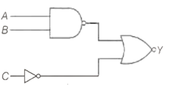

 Switch
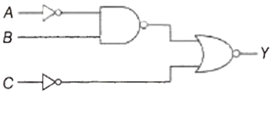

