Multiple Choice Questions
If a p-n junction diode of depletion layer width W and barrier height V0 is forward biased, then
W increases, V0 decreases
W decreases, V0 increases
both W and V0 increase
both W and V0 decrease
The heavily and lightly doped regions of a bipolar junction transistor are respectively
base and emitter
base and collector
emitter and base
collector and emitter
The circuit diagram shows a logic combination with the states of outputs X, Y and Z given for inputs P, Q, R and S all at state 1. When inputs P and R change to state 0 with inputs Q and S still at 1, the states of outputs X, Y and Z change to
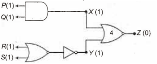
1, 0, 0
1, 1, 1
0, 1, 0
0, 0, 1
In a common emitter transistor amplifier, the output resistance is 500 kΩ and the current gain β = 49. If the power gain of the amplifier is 5 x 10⁶, the input resistance is
325 Ω
165 Ω
240 Ω
225 Ω
A transistor oscillator is
(i) an amplifier with positive feedback
(ii) an amplifier with reduced gain
(iii) the one in which DC supply energy is converted into AC output energy. Then
All (i), (ii) and (iii) are correct
(i) and (ii) are correct
(i) and (iii) are correct
(ii) and (iii) are correct
A pure semiconductor has equal electron and hole concentration of 1O16 m-3. Doping by indium increases nh to 5 x 10²² m-3. Then, the value of ne in the doped semiconductor is
106 /m3
1022 /m3
2 × 10⁹ / m3
1019 /m3
The collector supply voltage is 6 V and the voltage drop across a resistor of 6OO Ω in the collector circuit is 0.6 V, in a transistor connected in common emitter mode. If the current gain is 20, the base current is
0.25 mA
0.05 mA
0.12 mA
0.02 mA
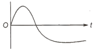
A full-wave rectifier circuit with an AC input is shown
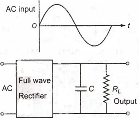
The output voltage across RL is represented as


 Switch