Multiple Choice Questions
In the operation of n-p-n transistor compared to that of a triode, the p base acts as
emitter
cathode
grid
plate
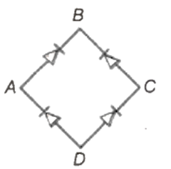
In the diagram, the input AC is across the terminals A and C. The output across B and D is

same as the input
half wave rectified
zero
full wave rectified
D.
full wave rectified
From the diagram, the input AC is across the terminals A and C. The output across B and D is full wave rectified.
A common emitter amplifier gives an output of 3 V for an input of 0.01 V. If β of the transistor is 100 and the input resistance is 1 kΩ, then the collector resistance is
1 kΩ
3 kΩ
30 kΩ
30 kΩ
When the forward bias voltage of a diode is changed from 0.6 V to 0.7 V, the current changes from 5 mA to 15 mA. Then its forward bias resistance is
0.01 Ω
0.1 Ω
10 Ω
100 Ω
In common emitter amplifier, the current gain is 62. The collector resistance and input resistance are 5 kΩ and 500 Ω respectively. If the input voltage is 0.1 V, the output voltage is
0.61 V
6.2 V
62 V
620 V
The current gain of a transistor in common base mode is 0.995. The current gain of the same transistor in common emitter mode is
197
201
199
202
The real time variation of input signals A and B are as shown below. If the inputs are fed into NAND gate, then select the output signal from the following


The time variations of signals are given as in A, B and C. Point out the true statement from the following


A, B and C are analogue signals
A and B are analogue, but C is digital signal
A and C digital, but B is analogue signal
A and C are analogue but B is digital signal
The energy gap between conduction band and the valence band is of the order of 0.7 eV. Then it is
an insulator
a conductor
a semiconductor
an alloy


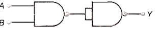
 Switch