 Multiple Choice Questions
In a semiconductor, 2/3rd of the total current is carried by electrons and remaining 1/3rd by the holes. If at this temperature, the drift velocity of electrons is 3 times that of holes, the ratio of number density of electrons to that of holes is
In an p-n-p transistor, 1010 holes enter the emitter in 10-6 s. If 29% of holes is lost in the base, then the current amplification factor is
49
19
29
39
The electrical conductivity of a semiconductor increases when electromagnetic radiation of wavelength shorter than 600 nm is incident on it. The energy band gap (in eV) for the semiconductor is
1.50
0.75
2.06
1.35
The inputs A, B and C to be given in order to get an output Y = 1 from the following circuit are

0, 1, 0
1, 0, 0
1, 0, 1
1, 1, 0
The light emitting diode (LED) is
a heavily doped p-n junction with no external bias
a heavily doped p-n junction with reverse bias
a heavily doped p-n junction with forward bias
a lightly doped p-n junction with no external bias
Identify the mismatched pair from the following
Zener diode : Voltage regulator
Germanium doped with phosphorus : n-type semiconductor
semiconductor : band gap > 3 eV
p-n junction diode : rectifier
In a common-emitter configuration, a transistor has β = 50 and input resistance 1 kΩ. If the peak value of AC input is 0.01 V, then the peak value of collector current is
0.01 µA
500 µA
100 µA
0.5 µA
The waveforms A and B given below are given as input to a NAND gate. Then, its logic output y is
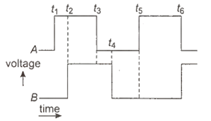
for t1 to t2 ; y = 0
for t2 to t3 ; y = 1
for t3 to t4 ; y = 1
for t4 to t5 ; y = 0
The logic gates giving output '1' for the inputs of '1' and 'O' are
AND and OR
OR and NOR
NAND and NOR
NAND and OR


 Switch

