Multiple Choice Questions
In an unbiased p-n junction
Potential at p is more than that at n
Potential at p is less than that at n
Potential at p is equal to that at n
Potential at p is +ve and that at n is −ve
In a common emitter amplifier the input signal is applied across
anywhere
emitter-collector
collector-base
base-emitter
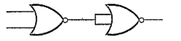
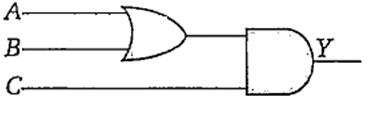
In the following combinations of logic gates, the outputs of A, B and C are respectively
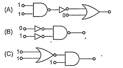
0, 1, 1
0, 1, 0
1, 1, 0
1, 0, 1
The forbidden energy gap in Ge is 0.72 eV, Given, hc = 12400 eV- . The maximum wavelength of radiation that will generate electron hole pair is
In a p-n junction diode not connected to any circuit
the potential is the same everywhere
the p-type side has a higher potential than the n-type side
there is an electric field at the junction directed from the n-type side to p-type side
there is an electric field at the junction directed from the p-type side to n-type side
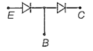
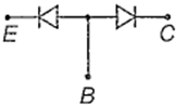
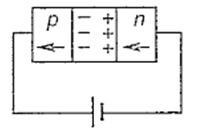
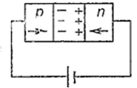
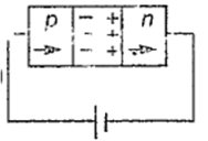
An n-p-n transistor can be considered to be equivalent to two diodes, connected. Which of the following figure is the correct one ?


In the case of forward biasing of a p-n junction diode, which one of the following figures correctly depicts the direction of conventional current (indicated by an arrow mark) ?


 Switch