CBSE Multiple Choice Questions
The following circuit represents

OR gate
XOR gate
AND gate
NAND gate
A forward biased diode is
![]()
![]()

Which one of the following represents forward bias diode?
In the combination of the following gates the output Y can be written in terms of inputs A and B as

![]()
![]()
![]()
![]()
In the circuit shown in the figure, the input voltage Vi is 20 V, VBE = 0 and VCE = 0. The values of IB, IC and β are given by

IB = 40 μA, IC = 10 mA, β = 250
IB = 25 μA, IC = 5 mA, β = 200
IB = 40 μA, IC = 5 mA, β = 125
IB = 20 μA, IC = 5 mA, β = 250
In forward biased if the p-n junctions diode is forward biased, then width of potential barrier in p-n junction diode
remains constant
increase
decrease
None of these
The following figure shows a logic gate circuit with two inputs A and B and the output C. The voltage waveforms of A, B and C are as shown below: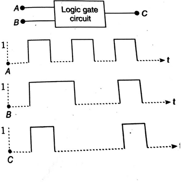
The logic curcuit gate is
AND gate
NAND gate
NOR gate
NOR gate
In a common emitter transistor amplifier, the audio signal voltage across the collector is 3 V. The resistance of collector is 3 kΩ. If current gain is 100 and the base resistance is 2 kΩ, the voltage and power gain of the amplifier is
200 and 1000
15 and 200
150 and 15000
150 and 15000
In a p-n junction diode, change in temperature due to heating
Affects only reverse resistance
Affects only forward resistance
Affects the overall V - I characteristics of p-n junction
Does not affect resistance of p-n junction
The given electrical network is equivalent to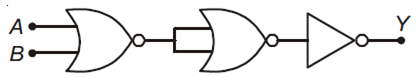
AND gate
NOR gate
OR gate
OR gate