CBSE Multiple Choice Questions
The energy band gap is maximum in
metals
superconductors
insulators
semiconductors
In a full wave rectifier, input AC current has a frequency v. The output frequency of current is
v
2 v
None of these
For a triode valve µ = 50, ΔVg = 0.2 V, then value of ΔVp is
5 V
10 V
0.2 V
50 V
n-type semiconductor is
positive charged
neutral
negatively charged
None of the above
A transistor is used in common emitter mode as an amplifier, then
the base emitter junction is forward unbiased
the base emitter junction is reverse biased
the input signal is connected in series with the voltage applied to bias of the base emitter junction
the input signal is connected in series with the voltage applied to bias the emitter collector junction
To get an output Y =1 from circuit of figure, the input must be

A = 0, B = 1, C = 0
A = 0, B = 0, C = 1
A = 1, B = 0, C = 0
A = 1, B = 0, C = 1
In a transistor circuit, the base current changes from 30 µA to 90 µA. If the current gain of the transistor is 30%, the change in the collector current is
4 mA
2 mA
3.5 mA
1.8 mA
Two identical p-n junctions may be connected in series with a battery in three ways as shown in the figure.
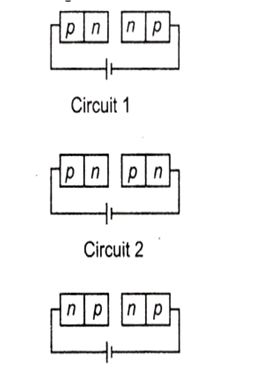
The potential drops across the two n-p junctions are equal in
circuit 1 and circuit 2
circuit 2 and circuit 3
circuit 3 and circuit 1
circuit 1 only
If dopping in the P region is high, then N region
depletion layer will be more towards P
depletion layer will be more towards N
depletion layer will remain unchanged
None of the above
A full wave rectifier circuit along with the output is shown in the figure. The contribution (s) from the diode 1 is ( are )
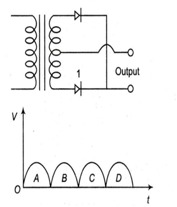
C
A , C
B , D
A, B , C , D