CBSE Multiple Choice Questions
A common emitter amplifier has a voltage gain of 50, an input impedance of 100 Ω and an output impedance of 200 Ω. The power gain the amplifier is
500
1000
1250
1250
To get an output Y = 1 from the circuit shown below, the input must be
|
A |
B |
C |
|
0 |
1 |
0 |
|
A |
B |
C |
|
0 |
0 |
1 |
|
A
|
B
|
C
|
|
1
|
0
|
1
|
|
A
|
B
|
C
|
|
1
|
0
|
1
|
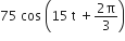
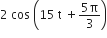
The input signal given to a CE amplifier having a voltage gain of 150 is 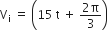 The corresponding output signal will be

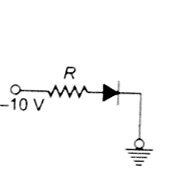
A Zener diode, having breakdown voltage equal to 15 V, is used in a voltage regulator circuit shown in the figure. The current through the diode is
10 mA
15 mA
20 mA
20 mA
In the following figure, the diodes which are forward biased, are


The device that can act as a complete electronic circuit is
Junction diode
Integrated circuit
Junction transistor
Junction transistor
Pure Si at 500 K has an equal number of the electron (ne) and hole (nh) concentrations of 1.5 x 10¹⁶ m-3.Doping by indium increases nh to 4.5 x 10²² m -3.The doped semiconductor is of
n- type with electron concentration ne = 5 x 10²² m -3
P- type with electron concentration ne = 2.5 x 10¹⁰ m -3
n- type with electron concentration ne = 2.5 x 10²³ m -3
n- type with electron concentration ne = 2.5 x 10²³ m -3
A transistor is operated in common emitter configuration VC = 2V such that change n the base current from 100 µA to 300 µA produces a change in the collector current from 10 mA to 20 mA. The current gain is
75
100
25
25
Which one of the following statement is false?
Pure Si doped with trivalent impurities given a p- type semiconductor
Majority carriers in a p- type semiconductor are holes
Minority carriers in a p- type semiconductor are electron
Minority carriers in a p- type semiconductor are electron
For transistor action
A) Base, emitter and collector regions should have similar size and doping concentrations.
B) The base region must be very thin and lightly doped.
C) The emitter-base junction is forward biased and base -collector junction is reverse biased
D) Both the emitter-base junction as well as the base-collector junction are forward biased.
(D) and (A)
(A) and (B)
(B) and (C)
(B) and (C)