CBSE Multiple Choice Questions
The potential barrier, in the depletion layer, is due to
ions
electrons
holes
forbidden band
When LED is forward biased, then
electrons from the n-type material cross the p-n junction and recombine with holes in the p-type material
electrons and holes neutralise each other
at junction electrons and holes neutralize each other
None of the above
Assertion: LASER is used to measure distant object as moon.
Reason: They are highly coherent source of light.
If both assertion and reason are true but reason is the correct explanation of assertion.
If both assertion and reason are true but reason is not correct explanation of assertion.
If assertion is true but reason is false.
If assertion is false but reason is true.
To a germanium crystal, an equal number of aluminium and indium atoms are added. Then
it remains an intrinsic semiconductor
it becomes a n-type semiconductor
it becomes a p-type semiconductor
it becomes an insulator
Identify the operation performed by the circuit given below
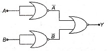
NOT
AND
OR
NAND
The electrical conductivity of semiconductor increases, when electromagnetic radiation of a wavelength shorter than 24800 Å is incident on it. The bandgap for the semiconductor is
0.9 eV
0.7 eV
0.5 eV
1.1 eV
In a transistor, the collector current is always less than the emitter current because
collector side is reverse biased and the emitter side is forward biased
a few electrons are lost in the base and only remaining ones reach the collector
collector being reverse biased attracts less electron
collector side is forward biased and emitter side is reverse biased
At 0 K temperature, a p-type semiconductor
does not have any charge carriers
has few holes but no free electrons
has few holes and few free electrons
has equal number of holes and free electrons
Assertion: Electric appliances with metallic body e.g., heaters, presses etc., have three pin connections, whereas an electric bulb has a two pin connection.
Reason: Three pin connections reduce heating of connecting cables.
If both assertion and reason are true and reason is the correct explanation of assertion.
If both assertion and reason are true but reason is not the correct explanation of assertion.
If assertion is true but reason is false.
If assertion is false but reason is true.
Assertion: During reverse biasing a diode doesn't conduct current.
Reason: It narrows the depletion layer.
If assertion and reason are true and reason is the correct explanation of assertion.
If both assertion andreason are true and reason is not the correct explanation of assertion.
If assertion is true but reason is false.
If assertion is false but reason is true.